Alpha: The History in Facts and Comments |
|||||||||||||||||||||||||||||||||||||||

|
Dig my grave both long and narrow
Make my coffin neat and strong (from an old American song) |
||||||||||||||||||||||||||||||||||||||
|
Contents Foreword Part 1. PDP and VAX Part 2. The PRISM Project Part 3. The Alpha Project Part 4. EV4, LCA4, EV45, LCA45 Part 5. EV5, EV56, PCA56, PCA57 Part 6. The Fall of DEC Part 7. EV6, EV67, EV68C, EV68A Part 8. The Epoch of Compaq Part 9. EV7, EV79, EV7z, EV8 Epilogue Additional Information Literature |
Paul V. Bolotoff
Release date: 14th of April, 2005 Last modify date: 19th of March, 2006 
|
||||||||||||||||||||||||||||||||||||||
|
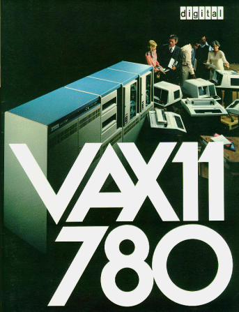
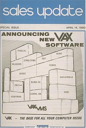
Foreword This work starts a set of articles dedicated to Alpha processors and the architecture, as well as to other areas connected. The set, because presenting the whole material available in a single overview would be somewhat problematic and generally inadequate from the author's point of view. Besides, the theme about to be opened is vast very much, fundamental in many aspects, and there are no preceding papers comparable to the author's one in means of fullness and scalability, taking into account all the architecture not separate products distanced significantly in time. Maybe this article would be looking better if was written and published several years ago, when Alpha processors were real kings considering performance, and their future was expected to be bright very much. However, only nowadays it seems to be the right time to draw the final line, to explain what happened, and why one of the most interesting and promising computer architectures has been thrown into oblivion. Generally, this paper is a historical overview with some elements of analysis, so it should be considered as such. It doesn't pretend to be universal though contains a real lot of reference information. On the other hand, it isn't a necrologue or a funeral prayer definitely... back to the contents Part 1. PDP and VAX Digital Equipment Corporation (abbreviated to DEC) was founded in 1957 by two engineers, Kenneth Olsen and Harlan Anderson, graduates of Massachusetts Institute of Technology, and was one of the oldest and most known companies of the world computer industry. Before founding, Olsen worked for Lincoln Laboratory at the institute mentioned above, which was supported by the Department of Defense [of the United States], and participated in development of one of the world's first transistor-based computers, TX-2. The company was producing and selling backplane modules for computers initially, but in 1960 it offered the first computer of its own, 18-bit PDP-1 (Programmable Data Processor - 1), capable of about 100 thousand operations per second. By the way, that machine was used to run the first computer game in known history, Spacewar of Steven Russell. 12-bit PDP-8, introduced in 1964, deserved to be called the first "minicomputer" (sized like a small wardrobe) manufactured in quantity. In addition, the price was attractive: about 18000 USD (1965) for the standardconfiguration. Because of an excellent price/performance ratio, PDP-8 was able to stand against those famous mainframe systems of IBM as a real competitor. There were about 1450 machines produced until 1968 (not counting numerous modifications following). 36-bit PDP-10 was ready in the same 1968, based upon the design of experimental PDP-6, and targeted for data processing centres, research laboratories, and military needs. Different versions of PDP-10 were manufactured until 1983. There were attempts taken towards improvements of that 36-bit architecture, organised within the Unicorn project under supervision of Leonard Hughes and David Rogers, but the project was closed in June of 1975, and all its resources were transferred to support another, 32-bit, architecture. 16-bit PDP-11 was launched in production in the beginning of 1970's. It was the first computer of DEC to feature use of 8-bit bytes, and a direct successor of the PDP-8 model line. Due to a simple and fortunate Unibus-based architecture (or a modified one, based upon Q-bus), a considerably effective instruction set, and low production costs, the model line of PDP-11 had faced a success. Quite obviously, PDP-11 became a subject of cloning actions all over the world, including even those "countries of people's democracy": CM-4 (the USSR, Bulgaria, Hungary), CM-1420 (the USSR, Bulgaria, the German Democratic Republic), CM-1600 (the USSR), IZOT-1016 (Bulgaria), DVK (the USSR). There were many operating systems developed for PDP-11: DEC offered P/OS, RSX-11, RT-11, RSTS/E, also several derivatives of DOS, and finally, the first release of UNIX OS was completed at Bell Laboratories on PDP-7 and PDP-11 machines in 1971 using their assembly languages. PDP-11 left the market during 1980's because of one, but inevitable reason: lack of address space. A new, 32-bit though still CISC, architecture was promoted to the market. So, that architecture was VAX (Virtual Address eXtension), approved officially during a VAX Architecture Committee session in April of 1975. The architecture was developed in several months while the Star project was operational and supervised by Gordon Bell, in parallel with the Unicorn project mentioned above. Upon completion of both the projects it was decided to cancel any further development of 36-bit systems, and to concentrate resources available to support 32-bit VAXen (the plural of VAX). In fact, the Star project was to prove the necessity of increasing general registers' width of PDP-11 to 32 bits, their number from 8 to 16, and a significant redesign of the instruction set. The first VAX machine was announced in October of 1977, model 11/780. A few months later, in February of 1978, was released a new operating system for VAXen, VMS (Virtual Memory System) v1.0. It was a multi-user and multi-tasking OS supporting up to 64Mb of main memory, networking functions (DECnet), an adaptive task scheduler, an extended process management, and many more innovations hard to be seen before. Renamed to VAX/VMS, v2.0 was presented in April of 1980, and carried numerous improvements over v1.0. In addition, the classical OS UNIX was ported to VAX soon. VAXen were manufactured and sold with a real success during 1980's, and were shipped in limited quantities under special contracts even when close to the end of the century. The whole model line included several dozens of kinds ranging from compact workstations to 6-processor mainframe-class servers. Even nowadays, thousands of VAXen keep working at subdivisions of the Department of Defense and the NSA (National Security Agency), also at numerous commercial organisations. Nevertheless, the epoch of VAXen was 1980's, at least because DEC made a bet on a new architecture in 1990's.
back to the contents Part 2. The PRISM Project In the beginning of 1980's, DEC was on the paramount of its financial wealth, mostly because of high revenues related to growing constantly sales of VAX machines. However, nothing lasts forever, and it was obvious that some day VAX would have to leave the market in favour of a new architecture as it was happening with PDP-11. Those days many companies started to pay more and more attention to RISC-based concepts and implementations, and DEC had no intention to ignore that trend. There were several subdivisions inside of DEC between 1982 and 1985, which researched actively over the RISC area:
In 1985, after Cutler's initiative on creating a so-called corporate RISC plan, all 4 projects were merged into one, PRISM (PaRallel Instruction Set Machine), and the first draft for a new RISC processor was released in August of 1985. To mention, DEC had participated in the development of MIPS R3000 processor those days and even initiated the creation of Advanced Computing Environment consortium to promote that architecture. No wonder that the processor inherited many features of the MIPS architecture during development, but at the same time the differences were obvious. All instructions were of fixed-length of 32 bits with the upper 6 and the lower 5 ones presenting an instruction code actually, and the remaining 21 were reserved for immediate data or addressing needs. There were 64 primary 32-bit general-purpose registers defined (MIPS supposed 32), also 16 additional 64-bit vector registers, and 3 control registers for vector operations: two 7-bit (vector length and vector count), and one 64-bit (vector mask). There was no processor state register, thus a result of two scalar operands compared was placed into a general-purpose register, but a result of two vector operands compared — into the vector mask. There was no built-in floating-point unit. A set of special instructions (Epicode, or Extended processor instruction code) was created in software [through loadable microcode] to facilitate handling of special tasks required for a particular environment or operating system given and not supported by the standard instruction set otherwise. Later, this function was implemented in the Alpha architecture under the name of PALcode (Privileged Architecture Library code). In 1988, when the project was still in progress, the high management of DEC decided to close it considering any further support as a waste of resources. Protesting against that decision, Cutler resigned and went to Microsoft to supervise a department developing Windows NT (called OS/2 3.0 those days). In the beginning of 1989, DEC presented first RISC-powered workstations of its own, DECstation 3100 with 32-bit MIPS R2000 inside clocked at 16MHz, and DECstation 2100 using the same processor type but clocked at 12MHz. Both the machines were running Ultrix OS and were priced rather inexpensively (about 8 ths. USD (1990) for DECstation 2100). back to the contents Part 3. The Alpha Project In 1989, the aging VAX architecture was hardly able to compete with RISC architectures of the 2nd generation such as MIPS and SPARC, and it was obvious that the next generation of RISC hardware would leave not so many chances to survive for VAX. In the middle of 1989, DEC's engineers had received a task to create a competitive RISC architecture with a long-term potential, but at the same time carrying a minimal set of incompatibilities with VAX. That was because VAX/VMS and all accompanying applications had to be ported to the new architecture, which was also defined to be 64-bit right from the start since competitors were about to release their 64-bit solutions. A development group was created with Richard Witek and Richard Sites involved as the chief architects. The Alpha architecture was mentioned officially for the first time on the 25th of February 1992 during a conference in Tokyo. In addition, most key features of the new architecture were listed within a concise overview (for comp.arch, a USENET conference). It was also mentioned that "Alpha" was an internal code-name and an official name would be provided later. The new processor was of a "clean" 64-bit RISC design to execute fixed-length instructions (32 bits every), with 32 integer 64-bit registers, operated with 43-bit virtual addresses (with a possibility to expand up to 64 bits in future implementations of the architecture). Like VAX, it used little-endian byte order (i.e. when a low byte of a register occupies a low memory address when stored, in contrary to big-endian byte order, introduced by Motorola and used in most processor architectures, when a low byte of a register occupies a high memory address when stored). A mathematical co-processor was built into the core together with 32 floating-point 64-bit registers which utilised random access order unlike primitive stack access order implemented in Intel x87 co-processors. The total lifetime of the new architecture was estimated in no less than 25 years. The instruction set was simplified to facilitate pipelining actions as much as possible and consisted of 5 groups:
To mention, there was no hardware support for integer divide instructions, because they would be the most computationally-expensive integer ones and thus badly pipelineable, so they were just emulated. It was acceptable, because this kind of instructions was needed relatively not so often in real life. Alpha architecture was a "real" RISC in contrary to modern processors of the x86 architecture which are RISC inside only. The conceptual difference between RISC (Reduced Instruction Set Computing) and CISC (Complex Instruction Set Computing) was (and still is) within a few moments:
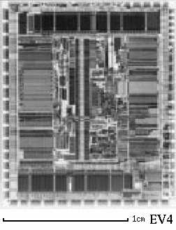
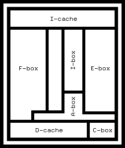
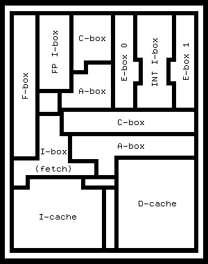
The processor was supposed to be launched in production at a very high core frequency — 150MHz which should be increased for up to 200MHz while utilising the same engineering limits. That appeared to be possible because of a successful architecture as well as because of the engineers' rejection to involve automatic design systems and doing all the work just by hands. The project entered manufacturing stage and was reorganised into a regular division of DEC soon. Because of DEC marketing department's efforts the new architecture was called AXP (or Alpha AXP), though still not known for sure what exactly this abbreviation meant. Quite possible that nothing at all: in the past, DEC had legal problems with its VAX brand because there was another pretending company, a manufacturer of vacuum cleaners, and that time the conflict was taken to court. By the way, it was also motivated that DEC's equipment sales suffered because of the other company's slogan, "Nothing sucks like a Vax!" After all, a joke had shown up saying that AXP meant "Almost Exactly PRISM" back to the contents Part 4. EV4, LCA4, EV45, LCA45 The first processor of the Alpha family was called 21064 ("21" implied that Alpha was an architecture of the 21st century, "0" — a processor's generation, "64" — a computational capability in bits), also code-named as EV4 ("EV" was [supposedly] the abbreviation of "Extended VAX" and "4" — a technical process' generation, CMOS4 — which, in turn, stood for Complementary Metal Oxide Semiconductor). To mention, a prototype of EV4 was ready in 1991 by using a less detailed CMOS3 process, therefore with the cache sizes reduced and with no floating-point unit. Nevertheless, it was an important threshold for tuning and polishing off the architecture and software environment. EV4 was introduced in November of 1992 and was manufactured using an advanced for those days 3-layer 0.75µ technological process (in the future, it was modified towards 0.675µ CMOS4S, the optical modification of CMOS4). Was designed for 3.3V supply and ith core frequencies ranging from 150MHz to 200MHz (TDP from 21W to 27W). Consisted of 1.68 mln. transistors and utilised a die size of 233mm². Supported multi-processing as one of the architecture's key features. Form-factor: PGA-431 (Pin Grid Array). The L1 cache was integrated: 8Kb for instructions (I-cache, instruction cache), direct-mapped, also 8Kb for data (D-cache, data cache), direct-mapped and write-through. Read latency of D-cache was 3 ticks. Every line of I-cache consisted of 32 bytes of instructions, a 21-bit tag record, an 8-bit branch history field, and of several auxiliary fields. Every line of D-cache consisted of 32 bytes of data and a 21-bit tag record. The L2 cache (B-cache, back-up cache) was a recommended option, using external synchronous or asynchronous SRAM chips, direct-mapped, write-back, write-ahead and sized up to 16Mb (from 512Kb to 2Mb usually). Every line consisted of 32 bytes of data or instructions with a 1-bit long-word parity or 7-bit long-word ECC field, a 17-bit maximum tag record with an additional 1-bit long-word parity protection, and a 3-bit condition flag with an additional parity bit. Read and write speeds of B-cache were programmable in the processor's ticks. The system data bus was either 64-bit or 128-bit wide (programmable, with a 1-bit long-word parity or 7-bit long-word ECC field) and was multiplexed with B-cache data bus, switched between if necessary. The system address bus was 34-bit wide. B-cache was organised to be inclusive to D-cache, i.e. contained a full copy of the latter. A mechanism called victim write was used to store data from B-cache to memory. The processor and no one else was able to perform read/write operations with B-cache, though the system logic was granted a permission to read B-tag data since it was of the top importance for multi-processor systems especially, to maintain cache coherence of all processors available within a machine. The processor was powered with one integer pipeline (E-box, 7 stages) and one floating-point pipeline (F-box, 10 stages). The instruction decoder and scheduler (I-box) was able to supply up to 2 commands per tick to the functional units, namely E-box, F-box, and load/store unit (A-box), in-order. The cache memory and system bus controller (C-box) worked in cooperation with A-box and supervised integrated I-cache and D-cache as well as external B-cache. Calculations of virtual addresses were handled by E-box. The branch prediction unit maintained a 4096-entry branch prediction table with 2 bits per entry. There was I-TLB (Instruction TLB) of 8 entries for 8Kb pages and 4 entries for 4Mb pages, also D-TLB (Data TLB) of 32 entries. Both of them were fully associative.
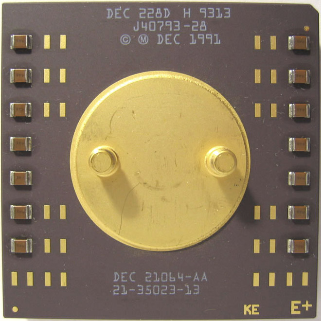
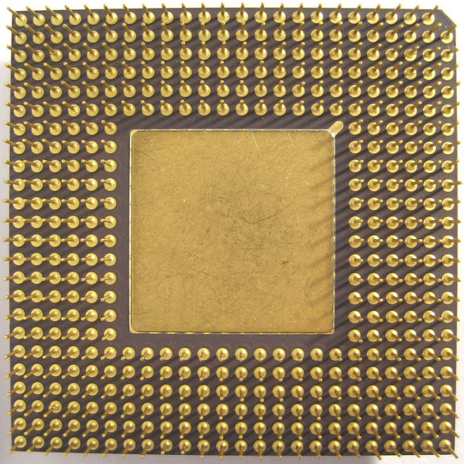
With a respect to its excellent performance, EV4 was expensive considerably for most potential customers, thus a low-priced brother was released in September of 1993, 21066 (LCA4 or LCA4S). It was based upon the core of EV4, but with memory and PCI controllers integrated additionally, also several secondary functional units. On the other hand, the system data bus width was reduced to 64 bits causing a negative impact on performance. LCA4 was manufactured using a 0.675µ CMOS4S process resulting in a die size even smaller than of original EV4 (209mm² compared to 233mm²). Additionally, its clock frequencies were lowered to range from 100MHz to 166MHz, presumably to avoid potential overheating issues common for ventilated badly desktop cases of those days, also to avoid creation of an additional competitor to EV4. Contained 1.75 mln. transistors and required 3.3V supply. The design of this processor was licenced to Mitsubishi, so it manufactured LCA4 as well (including a 200MHz version). 21064A (EV45) was announced at Microprocessor Forum in October of 1993. It was a modified EV4, produced using a 4-layer 0.5µ CMOS5 process. 21066A (LCA45) was presented at COMDEX in November of 1994. It was modified almost the same way as EV4 was towards EV45 but against LCA4. To mention, DEC's marketing people developed a habit to add a letter to a processor's model name after a redesign towards a more advanced technological process. Both the cores of EV45 and LCA45 were changed not so much: I-cache and D-cache of EV45 were doubled in size (16Kb I-cache + 16Kb D-cache) and their data and tag fields gained a parity bit each, branch history fields of I-cache were expanded to 16 bits, D-cache had become 2-way set associative, and 1-bit byte parity mode was added to those existing integrity modes of the system data bus. In addition, both EV45 and LCA45 were awarded with a modified F-box (division optimisation: EV4 could execute a floating-point division instruction in 34 ticks for single-precision operands and in 63 ticks for double-precision operands with no dependence upon operands' values; EV45 could do the same thing in 19 to 34 ticks for single-precision operands and in 29 to 63 ticks for double-precision operands, dependable upon operands' values). LCA45 was also manufactured by Mitsubishi. Both the dies were decreased in size: to 164mm² for EV45 and 161mm² for LCA45. The transistors' count increased to 2.85 mln. for EV45 and remained the same for LCA45 — 1.75 mln. Finally, power consumption per tick decreased for both the processors, though voltage didn't change from 3.3V. Core frequencies of EV45 ranged from 200MHz to 300MHz (TDP from 24W to 36W), of LCA45 — from 166MHz to 233MHz. DEC developed equipment for the Department of Defense (of the USA), so 21068 66MHz and 21068A 100MHz were introduced in 1994. They derived from LCA4 and LCA45 respectively, advanced for military needs (passive cooling, extreme temperature conditions asf.). First chipsets for EV4 featured support for TURBOchannel, FutureBus+ and XMI peripheral buses. Alhough all of them were high-speed designs for those days (about 100Mb/s per bus), they didn't obtain any significant support, thus a very limited set of peripherals was available for them. So, DEC paid certain attention to industry-standard bus architectures, such as PCI and ISA (EISA). A new chipset was introduced in 1994, DEC Apecs, in two editions: for 64-bit system data bus (21071) and for 128-bit one (21072). The difference was that 21071 consisted of 4 chips (1 universal controller — COMANCHE, 2 data slices — DECADE, 1 PCI bus controller — EPIC) but 21072 — of 6 (2 additional data slices). Supported 33MHz system bus frequency, up to 16Mb of B-cache, up to 4Gb of FPM parity memory with access time from 100 to 50ns (8 banks), and up to 16Mb of dual-ported VRAM for an optional video frame-buffer (1 bank). Support for the ISA or EISA buses could be implemented through use of standard bridges, such as i82378IB (ISA) or i82378EB (EISA). Had been used with EB64+ and AlphaPC 64 (code-named as Cabriolet) mainboard designs. The first workstation of Alpha architecture was available in November of 1992, DEC 3000 Model 500 AXP (code-named as Flamingo), with a 150MHz EV4, 512Kb of B-cache, 32Mb of main memory, integrated 8-bit video controller with 2Mb of VRAM, 1Gb SCSI HDD, SCSI CD-ROM, built-in 10Mbit Ethernet controller (thick coaxial and twisted pair), built-in sound and ISDN controllers, also a 19" monitor (1280x1024x72Hz). The price was impressive very much: 39 ths. USD. In July of 1994, two EV45-based workstations had been announced: DEC 3000 Model 900 AXP and Model 700 AXP (code-named as Flamingo45 and Sandpiper45 respectively). The first one was powered with a 275MHz processor, but the second one — with a 225MHz. Both of them were accommodated with 2Mb of B-cache, 128Mb of main memory, a ZLX family 24-bit video card, FastSCSI peripherals, and the same networking, sound, and ISDN hardware to of Model 500 AXP. The first workstation was offered for 43,4 ths. USD, the second — for 27,7 ths. USD. 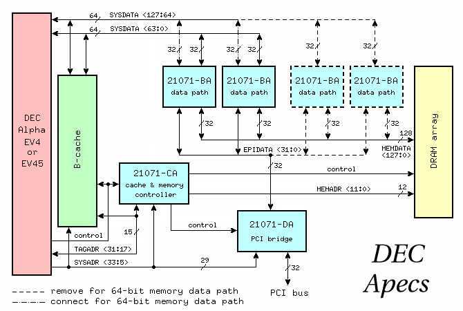
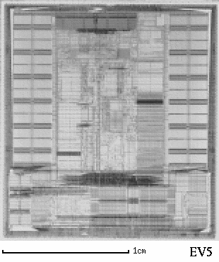
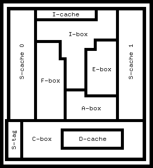
back to the contents Part 5. EV5, EV56, PCA56, PCA57 DEC had unveiled the very first information about the 2nd generation Alpha processor at Hot Chips conference located in Palo Alto (California), which started on the 14th of August 1994. Although the official release of 21164 (EV5) was dated by the 7th of September 1994, after a respective press release by DEC. The processor was based upon the core of EV45 and was rather an evolution of the latter than a revolutionary new design. The number of pipelines was doubled, both integer and floating-point, when compared to EV4 or EV45. In addition, the floating-point pipelines were transformed to run through 9 stages rather than 10. Additionally, the integer pipelines weren't all the same if compared to each other: while both were capable of elementary arithmetical and logical operations, the 1st only could multiply and shift, and the 2nd only was able to process conditional/unconditional branches. Both the pipelines could calculate virtual addresses for load instructions, but the 1st one only — for store. The floating-point pipelines were different as well: the 1st could execute any floating-point code except of multiply instructions, which were the only code the 2nd pipeline could process. I-box was able to fetch and decode up to 4 instructions per tick to provide the execution units with a proper load. Was manufactured using the same 4-layer 0.5µ CMOS5 process as EV45, required 3.3V supply, contained 9.3 mln. transistors (including 7.8 mln. for integrated cache areas), utilised a die size of 299mm² — very close to theoretical limits of the technical process involved. Core frequencies ranged from 266MHz to 333MHz (TDP from 46W to 56W). Form-factor: IPGA-499 (Interstitial Pin Grid Array). I-cache and D-cache were sized and organised just like in EV4, i.e. 8Kb each. D-cache remained write-through but was made dual-ported, i.e. was able to deliver data for 2 load instructions per tick. Sacrificing transistors for the sake of performance, D-cache was composed physically of 2 identical absolutely parts of 8Kb each, so data could be read from either one, but had to be written to the both. The processor was accommodated with 96Kb of the integrated L2 cache (S-cache, secondary cache), write-back, 3-way set associative, and C-box was made able of utilising it through a dedicated 128-bit data bus. At the same time, B-cache was also functional though remained optional, consisted of external cache SRAMs and could be as large as 64Mb, though usually from 1Mb to 4Mb — in other words, EV5 supported 3 cache levels. S-cache was accessed through a 4-stage pipeline: two ticks for tag search and modification plus two ticks for data access and delivery. Every S-cache line was 64 bytes wide with one tag per line, though it was possible to address every line as of two sublines 32 bytes wide each. Read latency of D-cache was reduced from 3 to 2 ticks, and S-cache could deliver data in 7 ticks (like mentioned above, 4 ticks for the first set of 16 bytes and 1 tick for every next set of 16 bytes to fill a whole line). Like in EV4, contents of D-cache were doubled, but in S-cache this time. In turn, B-cache was inclusive to S-cache regardless of the difference in associativities. I-TLB held 48 entries (for pages sized from 8Kb to 4Mb), D-TLB — 64 entries, and it had become dual-ported for reading like D-cache. The system data bus was fixed-length at 128 bits with additional 16 bits for ECC protection, still multiplexed with the data path to B-cache. The system address bus was 40-bit, the control — 10-bit.
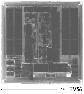
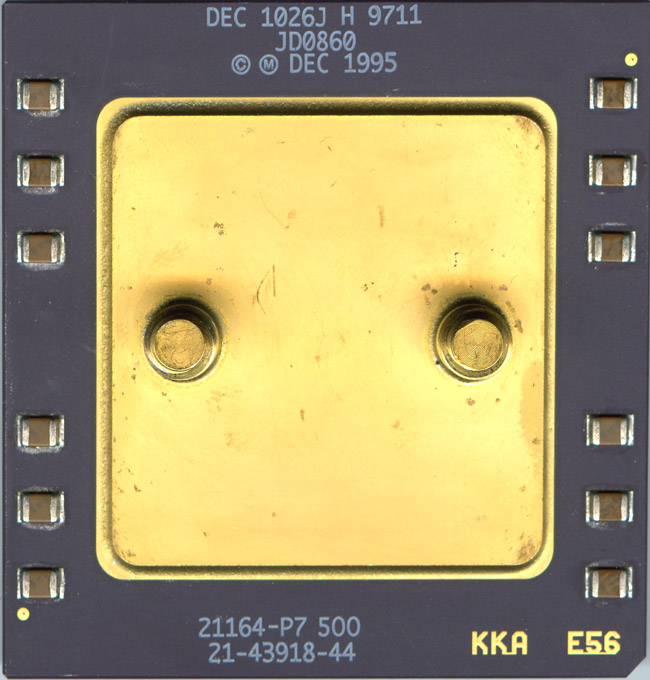
21164A (EV56) was introduced at Microprocessor Forum in October of 1995. It was a modified release of EV5, after a technology shrink to a 4-layer 0.35µ CMOS6, manufactured at the same factory in Hudson (DEC had invested about 450 mln. USD prior to in modernisation). The most important architectural difference was BWX (Byte-Word Extension) — a set of 6 additional commands to load/store data in 8- or 16-bit quanta. Right from the start, the Alpha architecture was forced to load/store data in 32- or 64-bit quanta, what caused certain difficulties while porting or emulating code belonging to other processor architectures, such as i386 or MIPS. A request to implement BWX in hardware was submitted in June of 1994 by Richard Sites and was approved in June of 1995. Although to utilise BWX a chipset should be aware of it as well. EV56 was manufactured with core frequencies ranged from 366MHz to 666MHz (TDP from 31W to 55W), starting from the summer of 1996. Also was produced by Samsung under a licence agreement signed in June of 1996 (a 666MHz version was shipped from Samsung only). Contained 9.66 mln. transistors, utilised a die size of 209mm² and required dual voltage (2.5V for primary and 3.3V for input-output circuits).
21164PC (PCA56) was introduced on the 17th of March 1997. It was a low-cost version of EV56 designed by DEC and Mitsubishi cooperatively. S-cache was absent as well as accompanying logic, but I-cache size was increased by factor of two (to 16Kb). Contained 3.5 mln. transistors, utilised a die size of 141mm², also the same technical process and voltage as EV56, but the form-factor did change: IPGA-413 instead of IPGA-499. Core frequencies ranged from 400MHz to 533MHz (TDP from 26W to 35W). In the future, 0.28µ 21164PC (PCA57) was manufactured by Samsung, with I-cache and D-cache doubled in size, also with 2-way set associativity of D-cache. The transistors' count increased to 5.7 mln. but the die size decreased to 101mm² at the same time. Required lower voltages: 2.0V for primary and 2.5V for input-output logic. Core frequencies ranged from 533 to 666MHz (TDP from 18W to 23W). In addition to BWX (inherited from EV56), PCA56 and PCA57 supported a new instruction set, MVI (Motion Video Instructions), targeted to accelerate video and audio calculations using SIMD (Single Instruction — Multiple Data) approach, somewhat comparable to the MMX instruction set for i386 processors. The first standard chipset developed for EV5 was DEC Alcor (21171). It supported a 33MHz system bus, up to 64Mb of B-cache, up to 8Gb of main memory (FPM ECC, using a 256-bit wide memory data path), also a 64-bit PCI bus at 33MHz. Support for either the ISA or EISA bus could be added through use of a standard bridge like before. There was no built-in IDE controller, which could be installed separately using a third-party hardware. The chipset consisted physically of 5 chips: 1 universal controller with the PCI bus support (Control, I/O and Address — CIA) and 4 data switches (DSW). A new release of Alcor was completed after launching EV56 in production — Alcor 2 (21172), which featured the BWX support. It was followed soon by Pyxis (21174), a single-chip solution supporting 66MHz system bus and 66MHz SDRAM ECC memory accessed through a 128-bit wide memory path. There was also VLSI Polaris developed for PCA57-based systems. back to the contents Part 6. The Fall of DEC On the 26th of January 1998, a news flashed all over the computer world that struggling financially DEC was purchased by Compaq Computer Corporation, and the deal was about to be approved by the upcoming shareholders' meetings of both the companies. DEC's shareholders ratified the agreement on the 2nd of February 1998. The amount of sale was 9.6 mlrd. USD, compared to DEC's estimated market capitalisation of about 7 mlrd. USD. The process of integrating DEC's functional units into Compaq's business structure was finished about half a year later with the legal end of DEC, when its shares were taken off the New York Stock Exchange on the 11th of June 1998. To mention, negotiations between DEC and Compaq started in 1995, but finished unsuccessfully in 1996 because DEC's high management held a position insisting on a merger, not on an acquisition. Nevertheless, here comes a question: how could it happen that a huge company (in figures of 1989: almost 130 thousand of personnel, gross revenue of about 14 mlrd. USD per year, i.e. the second company in the industry after IBM), which held a very high R&D potential and significant manufacturing facilities, was forced to sell itself to a large computer-building company from Texas? There was no definite answer to this question, though reasons mentioned were various. About them in detail. A long time ago, Kenneth Olsen, a founder, president and CEO of DEC until almost the end, said that well-engineered products would sell themselves. Thus, have no need in any advertising campaigns or other instruments of market promotion. He also mentioned that there is no reason anyone would want a computer at home. Perhaps, these thoughts were correct in those "old good times", when computer equipment was manufactured in limited quantities by professionals and for professionals, thus cost a hefty amount per unit. However, they weren't appropriate somewhere close to the end of the 20th century, when computer equipment was sold in million units per year, and a very regular computer could be taken together using a screwdriver and parts from the nearest computer shop for an hour maximum, besides it would cost over 10 times less than a big one mentioned previously. Finally, nothing should prevent from purchasing a whole working box right from that shop with a free delivery. Considering that such a regular machine would be purchased most likely not by a professional manager, realising clearly what TCO (Total Cost of Ownership) means, but by an aunt Marge or a young prankster Johnny, making no difference between a transistor and a resistor, so such customers should be motivated definitely not by engineering advantages of a potential purchase. Mistake #1. When at the very beginning of the Alpha architecture's way, DEC's high management made a great strategic mistake. It was a known fact that first prototypes of EV4 were presented on a computer conference in February of 1991. Among others, there were engineers of Apple Computer admitted, looking for a new processor architecture to power company's future computers, and they were impressed by advantages of EV4. John Sculley, Apple's CEO of those days, met with Kenneth Olsen in June of the same year and offered him to use the new processor of DEC in future Macs. Olsen refused the offer motivating that the processor was not ready for the market, besides the VAX architecture hadn't reached its end-of-life yet. Several months later, rumours said that new Macs would be powered by PowerPC processors from the alliance of Apple, IBM and Motorola. William Demmer, a former vice-president of VAX and Alpha divisions who resigned in 1995, said later in his interview to the Business Week (the 28th of April 1997): "Ken did not want the company's future to run on Alpha." Mistake #2. DEC manufactured Alpha processors as well as accompanying chipsets and numerous peripherals at its own factory in Hudson (Massachusetts). It designed and produced OEM- and retail-available mainboards for desktops and workstations only (they were even called so, Evaluation Board or AlphaPC), in a limited assortment though. Neither of them supported SMP, though almost all Alpha servers by DEC were multi-processors. Nevertheless, all mainboards were very well-engineered, though expensive like Alpha processors. Their layout schemes were available for public access, so several companies (Aspen, Polywell, Enorex asf.) manufactured fully qualified clones. The only company to develop and produce stand-alone designs was DeskStation. In general, it could be stated for sure that DEC considered a priority to produce workstations and servers of its own, but not to fill the market of computer components for those workstations and servers mentioned. It's possible to survive by following such an approach, but not possible to conquer the market and to promote the architecture to masses. Mistake #3. Despite all attempts taken, DEC didn't manage to make pricing of its products (considering processors, chipsets and mainboards first) affordable to most potential customers. For example, 266MHz and 300MHz EV5 were offered in the beginning of 1995 for 2052 and 2937 USD respectively in lots of 1000 units — both the enormous prices even taking into account average manufacturing costs (estimated) of 430 USD per unit. Considering price per one "parrot" of SPECint92, EV5 cost about 2 times higher than competitive RISC designs! At the same time, a standard chipset for EV5 (Alcor) was offered much cheaper — 295 USD in lots of 5000 units, though the only Alcor-based mainboard from DEC (EB164 with 1Mb of B-cache), bundled with a processor and 16Mb of main memory (by the way, that was not enough to run most applications even of those days), carried a list price of about 7500 USD. Mistake #4. Although Alpha was declared an open architecture right from the start, there was no consortium to develop it. All R&D actions were handled by DEC itself, in cooperation with Mitsubishi sometimes. In fact, though the architecture was free de jure, most important hardware designs of it were pretty much closed de facto, and had to be paid-licenced (if could be at all). So, it wasn't that thing helping to promote the architecture. To mention, soon after introduction of EV4, DEC's high management offered to licence manufacturing rights to Intel, Motorola, NEC and Texas Instruments. But all these companies were involved in different projects and were of a very little to no interest in EV4, so they refused. Perhaps, the conditions could be also unacceptable or something else. Mistake #5. After all, even the fastest computer without an operating system and accompanying software is just an expensive source of noise and an environmental heater. DEC targeted its Alpha hardware for Windows NT, Digital UNIX and OpenVMS, following this priority order exactly. Could be not bad, but... Windows NT was an operating system designed for users when right out-of-the-box, not for programmers (no software development tools supplied), hence dependent heavily upon precompiled applications, commercial notably. In fact, numbers of Alpha-ready and i386-ready software titles were different by a few times. Although there was FX!32, an excellent emulator and translator of x86 code to Alpha, completed by Anton Chernoff's team in 1996. While being a useful solution itself, couldn't help with performance decrease of 40% at least, when compared to the same source code compiled natively. Next, there were drivers, and FX!32 was absolutely of no help there. Considering a fact that very few hardware manufacturers honoured the Alpha architecture enough to release any of them, users had to rely mostly upon Microsoft and DEC. Finally, Windows NT (3.51 as well as 4.0) was a 32-bit OS regardless of running on the 64-bit Alpha hardware, thus was unable of utilising it to the full extent. However, all these issues didn't prevent DEC to promote its Alpha systems with a slogan "Born to run Windows NT". In brief, such an OS shouldn't be positioned as the primary for the Alpha architecture, though having it available as an option was a big plus for the architecture, especially on the workstation market. Mistake #6.
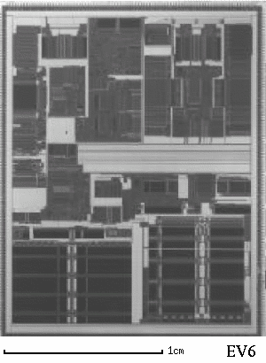
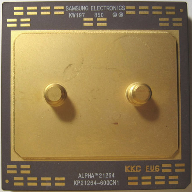
The list of DEC's strategical mistakes could be continued, including a complete disregard paid to the revolution of mass and cheap personal computers, an over-diversified business model, and others less important and unrelated directly to the Alpha architecture. Therefore, the final conclusion could be derived from the author's point of view: DEC had done a real number of efforts to make as much money as possible with the Alpha architecture, but had done almost no efforts to help the architecture itself. The board of directors, motivated by numerous company's failures during the late 1980's and early 1990's, suspended Olsen from managing the corporation in June of 1992 and appointed Robert Palmer instead. He did a hard try to reorganise the company's managing model in 1994 turning the existing "matrix" model (when departments different functionally cooperated to make a decision) into a traditional "vertical" (with authorities and responsibilities defined clearly from the very top to the very bottom of a company). From 1991 to 1994, DEC's net losses figured into over 4 mlrd. USD including 2 mlrd. just from July of 1993 to June of 1994 (in turn, including 1.2 mlrd. spent for restructurisation). The number of personnel was reduced to 85 thousand. Accordingly to Palmer's programme, the company should get rid of many divisions considered non-priority, so the global sale began. In July of 1994, the Storage Business Unit (manufacturing disk and tape drives) was sold to Quantum for 400 mln. USD, soon after a fiasco of the first models of thin-film hard drives (RA90 and RA92), which entered the market too late because of design flaws and didn't survive in competition. In August of 1994, the Database Software Unit was sold to Oracle for 100 mln. USD, also a 7.8% share in Italian Olivetti was redeemed for 140 mln. USD. In November of 1997, a deal was arranged to transfer the Network Product Business Unit to Cabletron for 430 mln. USD. The fall of DEC was loud enough. It sued Intel in May of 1997 accusing in infringements upon 10 patents issued for the Alpha architecture while designing Pentium, Pentium Pro and Pentium II processors. Intel started a lawsuit against DEC in September of 1997 claiming its 14 patents to be dishonoured while designing Alpha processors. The peace was reached finally on the 27th of October 1997: both the companies took their complaints back, DEC licenced to Intel manufacturing rights for all its hardware available (except of the Alpha segment), also agreed to support the future IA-64 architecture, and Intel purchased from DEC the factory in Hudson accompanied with designing centres in Jerusalem (Israel) and Austin (Texas) for 625 mln. USD, also agreed to manufacture DEC's Alpha processors in the future. Additionally, an agreement was signed to cross-licence their patents for 10 years. The deal was finished on the 18th of May 1998; by that time, Compaq had adopted DEC's primary divisions employing 38 thousand of personnel compared to 32 thousand of Compaq before the acquisition, though many of them were laid off in the very near future. Well to mention, not so long before the end of DEC and soon after that, many leading engineers who created DEC's realm in fact, left for other employers: Derrick Meyer quit to AMD to design K7; also to AMD, but as an architect of K8, went James Keller; Daniel Leibholz was hired by Sun to create UltraSPARC V; Richard Sites, one of primary Alpha architects during all the previous years, also abandoned the ship. Intel was lucky much less: the StrongARM architecture (inherited from DEC) seemed to be at a dead end because no one of those chief architects who designed StrongARM-110 previously, such as Daniel Dobberpuhl, Richard Witek, Gregory Hoeppner and Liam Madden, decided to join the new owner. More about that: Witek's team, which worked in Austin towards the 2nd generation of the StrongARM core, resigned completely, so Intel had to design the core from the scratch literally, involving engineers of its own who worked on i960 before. back to the contents Part 7. EV6, EV67, EV68C, EV68A Although 21264 (EV6) processor was developed by DEC and was mentioned first at Microprocessor Forum in October of 1996, the final silicon implementation was done by February of 1998, when DEC was in process of liquidation. The processor itself was a significant step forward when compared to EV5, revolutional in many aspects. One of the most important innovations was out-of-order execution, which implied a fundamental core redesign and lowered functional units' dependence upon cache and main memory's bandwidth. EV6 could reorder up to 80 instructions on the fly, and that was much more than other competitive products could (say, Intel's P6 architecture utilised out-of-order execution for up to 40 [micro-commands], HP PA-8x00 — up to 56, MIPS R12000 — up to 48, IBM POWER3 — up to 32, but PowerPC G4 — up to 5; Sun UltraSPARC II didn't support instruction reordering at all). Out-order-execution was supported by register renaming technique, so there were 48 integer and 40 floating-point additional physical registers implemented (the number of logical registers, also referred as programmable, remained unchanged — 32 integer and 32 floating-point). The number of integer pipelines was increased to 4 (organised in 2 clusters), but they were somewhat different functionally: the 2nd pipeline was capable of multiplying (7 ticks per instruction) and shifting (1 tick), the 4th — of executing MVI code (3 ticks) and shifting. Besides, all 4 pipelines supported elementary arithmetical and logical operations (1 tick). Every cluster featured an integer register file of its own (80 entries, like mentioned above), but they were identical (synchronised). The 1st and the 3rd pipelines also handled some tasks of A-box by calculating virtual addresses for load/store instructions. A-box itself worked with I-TLB and D-TLB (128 entries each), load and store queues (32 commands each), also 8 64-byte buffers (miss address file) for transactions with B-cache and main memory. Floating-point pipelines were different functionally as well: the 1st supported adding (4 ticks), dividing (12 ticks for single-precision and 15 ticks for double-precision), square root calculating (15 and 30 ticks), but the 2nd was only capable of multiplying (4 ticks). By the way, square root calculating unit and instructions related were new to the Alpha architecture. Like before in EV5, decoder was able to process up to 4 instructions per tick, and scheduler separated them for 2 queues: to integer pipelines (I-queue, 20 commands) and floating-point pipelines (F-queue, 15 commands). Behind of square root calculations, prefetch instructions were implemented as well as commands to transfer data between integer and floating-point registers. C-box was redesigned significantly and was capable of supporting only 2 cache levels. The integrated L1 consisted of 64Kb I-cache and 64Kb D-cache, both 2-way set associative and with 64-byte lines. D-cache was write-back, though still was doubled in B-cache. Because of a large size and more complicated associativity policy, D-cache read/write latencies were increased to 3 ticks (to/from an integer register) and 4 ticks (to/from a floating-point register). D-cache remained dual-ported, though unlike in EV5 it wasn't of 2 equal synchronised parts, but of a single part clocked at double the core frequency. External B-cache of 1Mb to 16Mb, direct-mapped, write-back, utilised an independent 128-bit bidirectional data bus (with an additional 16-bit ECC protection), also an independent 20-bit unidirectional address bus. B-cache consisted of LW SSRAM chips (late write), later of DDR SSRAM units (double data rate). B-cache's speed was programmable from 2/3 to 1/8 of a core frequency. Unlike for the previous generations of Alpha processors, B-cache itself wasn't optional. The system data bus was only 64-bit wide with an additional 8-bit ECC protection, bidirectional, but utilised the DDR technique. The system address bus was 44-bit wide, implemented physically through two 15-bit unidirectional paths with no DDR support. The system control bus was 15-bit, also with no DDR support. The basic working principle of the system bus was changed, so the bus became dedicated instead of shared, thus every processor possessed an own path to a chipset. The branch prediction logic was redesigned completely. It followed a 2-level scheme: with a local history table of 1024 records 10-bit each, and a local predictor of 1024 records 3-bit each, also with a global predictor of 4096 records 3-bit each, and a history path of 12 bits. Both the algorithms worked independently, and if the local one traced every branch available, the global one traced sequences of branches. The chooser analysed results of both the algorithms and made conclusions to a separate choice predictor of 4096 records 2-bit each, which was the source of a preferred decision if the predictions were different. Such a cooperative approach allowed to achieve better results than any of both of them if used stand-alone. While engineering EV6, considering a large number of advanced functional units and other complications, the clock subsystem was redesigned entirely. A more efficient signal flow allowed the core to reach frequencies of the much simpler core of EV56 while involving almost the same technological process. Overall, power consumed by the clock subsystem of EV6 was about 32% of the total core power. To compare, for EV56 it was about 25%, for EV5 — about 37%, for EV4 — about 40%. 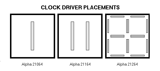
EV6 was manufactured using the same technological process to of EV56, but with 2 additional metallisation layers. Consisted of 15.2 mln. transistors (including about 9 mln. spent for I-cache, D-cache and branch predictors), utilised a die size of 314mm² and required 2.1V to 2.3V supply. The core frequencies ranged from 466MHz to 600MHz (TDP approx. from 80W to 110W). Form-factor: PGA-587 (Pin Grid Array).
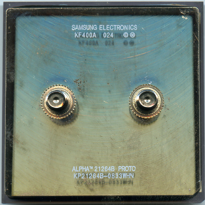
21264A (EV67) entered the market in the end of 1999. Produced by Samsung using a 0.25µ CMOS7 process, posessed a die size of 210mm² and required a lower supply of 2.0V. No architectural differences compared to EV6. The core frequencies ranged from 600MHz to 833MHz (TDP approx. from 70W to 100W), which allowed Alpha to bring back the leadership on integer tasks, lost not so much time ago to Intel Pentium III and AMD Athlon. The first samples of 21264B (EV68C) were delivered in the beginning of 2000. It was produced by IBM using a 0.18µ CMOS8 process involving copper conductors. Despite absence of any architectural differences still, the promising technology allowed to increase core frequencies right up to 1250MHz. In 2001, Samsung was able to manufacture 21264B (EV68A) in series using a 0.18µ process of its own, but involving aluminium conductors, thus reducing the die size to 125mm² and voltage to 1.7V, which allowed to place core frequencies in between 750MHz and 940MHz (TDP approx. from 60W to 75W). It was declared in September of 1998 that EV68 from Samsung would be implemented in an innovative 0.18µ FD-SOI (Fully Depleted Silicon-On-Insulator) process involving copper conductors, which should allow EV68 to reach 1.5GHz and even more. Unfortunately, it didn't happen.
Different sources mention 21264C and 21264D, code-named as EV68CB and EV68DC, manufactured by IBM using the same technology as EV68C and running within the same frequency range, so they could be considered as minor modifications. The only noticeable difference was a new form-factor, pinless CLGA-675 (Ceramic Land Grid Array) instead of PGA-587. There were 2 chipsets designed initially for processors of 21264 series: DEC Tsunami (21272; also known as Typhoon) and AMD Irongate (AMD-751), though could be many more if to take into account that both 21264 and Athlon utilised almost the same system bus, which had been licenced by DEC to AMD. DEC Tsunami was a highly scalable chipset. It could be used to design single-processor as well as dual-processor and quad-processor systems with the memory path from 128 to 512 bits wide (SDRAM ECC registered, 83MHz) and supporting from one to several PCI buses (64-bit, 33MHz). Such a flexibility was reached because of chipset separation for components: system bus controllers (C-chips, one per processor), memory bus controllers (D-chips, one per every 64 bits of the bus width) and PCI bus controllers (P-chips, one per bus needed). So, there is no wonder that some systems (for example, AlphaPC 264DP) were provided with chipsets consisting of 12 chips... Although AMD Irongate (AMD-751) was developed to serve as a north bridge to Athlon-based mainboards, accompanied with the AMD Viper (AMD-756) south bridge or a compatible one, it was used in some Alpha mainboards (to be precise, in UP1000 and UP1100). Being a single-chip solution, it cost much less than DEC Tsunami and consumed much less energy. However, it wasn't the best solution for 21264, because lacked multi-processing support and had a narrow memory path (64-bit, SDRAM ECC unbuffered, 100MHz). Nevertheless, Irongate was the first chipset for Alpha to feature the AGP bus support. In 2001, Samsung introduced the UP1500 mainboard, which was a single-processor solution designed upon the AMD Irongate-2 (AMD-761) north bridge. This mainboard was superior in means of performance to UP1000 and UP1100 due to support of a more advanced operating memory technology: Irongate-2 could utilise either up to 4Gb of DDR SDRAM ECC registered at 133MHz in 4 DIMMs with 2 RAS lines each or up to 2Gb of DDR SDRAM ECC unbuffered at the same 133MHz in 2 DIMMs with 2 RAS lines each. However, the memory path remained narrow (64-bit), and less expensive unbuffered ECC memory as well as non-ECC memory didn't seem to be supported by the firmware of UP1500. back to the contents Part 8. The Epoch of Compaq In fact, Compaq purchased the remains of DEC because of significant assembling facilities, its wide distributional network (in 98 countries) and that cross-licensing agreement with Intel (for example, allowing to manufacture 8-processor Profusion servers). As it seemed to be, the division developing the Alpha architecture wasn't welcome really: Compaq produced workstations and servers based upon Intel's processors for a very long time and also paid a high attention to AMD's processors. So, in June of 1998, Compaq established an alliance with Samsung to develop the architecture (to mention, DEC and Samsung signed an agreement in February of 1998, which gave a full access to all Alpha-related patents to the latter, allowed to manufacture the Alpha processors developed already and even to design new ones on Samsung's own). A new company was incorporated mutually, API (Alpha Processor Inc.), to promote the architecture (some ones seemed to make right conclusions based upon DEC's history). In the summer of 1998, EV6-based systems entered mass production stage featuring the best price/performance ratios compared to other competing products available on the market. Serious problems with future Itanium from Intel were reasonable enough to conclude that the situation described would remain unchanged in the near future. Outside of Samsung, the EV6 processors were manufactured by Intel using its Fab-6 in Hudson, accordingly to the final agreement with late DEC... Year 1999 was unsuccessful to Compaq because of falling sales on the market of personal computers. The most frequently named reason was an underestimation of possibilities given by the Internet to promote and sell PCs. Unlike Dell, which adapted its business model and offered computer equipment priced most attractively among all top brands. Compaq's CEO, Eckhard Pfeiffer, resigned after a financial disaster in the 1st quarter of 1999. Trying to reduce losses, Compaq started to minimise its presence in certain areas and that affected Alpha systems: in May of 1999, an assembling line of AlphaServers in Salem (New Hampshire) was announced to shut down soon. On the 23rd of August 1999, a notorious event took place: Compaq announced to discontinue participation in development of Windows NT and stopped to supply this OS with Alpha systems of its own. In fact, it also laid off a team of about 120 programmers from former Western Research Laboratory of DEC (DECwest) working on this project. Accordingly to Compaq's statistics, among all preinstalled operating systems on new Alpha machines Tru64 held a share of 65%, OpenVMS — of 35% and Windows NT just about of 5%, so there was no reason to keep flogging a dead horse. A week after, Microsoft announced in return that there would be no Windows 2000 for Alpha released. Considering a fact that support of PowerPC and MIPS architectures was abandoned by Microsoft in 1997 together with Motorola and SGI respectively, the future of "the universal OS" was sentenced to be tied to a single architecture if to discount IA-64... In December of 1999, Compaq and Samsung signed a memorandum to support the leadership of the Alpha architecture in the near future. Both the sides agreed to invest 500 mln. USD into the architecture (Samsung was obligated to spend 200 mln. USD into development and tuning of new technical processes, and Compaq was supposed to spend 300 mln. USD into design of new server solutions and further development of Tru64 UNIX). In addition, during the same month Compaq and IBM agreed that the latter would manufacture Alpha processors using a copper-conductor technology of its own upon completion. At the same time, Samsung was granted to remain the primary supplier of Alpha processors. The year passed not so good for Compaq illustrated well by a price per share delta: from 51 USD in February to 28 USD in December. Though many analysts stated it could be worse. Y2K passed for Compaq quietly. Samsung wasn't able to tune its 0.18µ process unlike IBM, which started to supply EV68C to Compaq in limited quantities, and the market had to enjoy considerably slow EV67. The development of 21364 (EV7, also known as Marvel) was in progress still, though 21464 (EV8, also known as Araña) was mentioned here and there. The fall of dot-coms affected Compaq's shares, which dropped in price to 15 USD per share by December, i.e. for 44% since January. Could be strange, but that was a good result; other companies, more depend�ble upon e-commerce, lost much more: Gateway — 75%, Apple — 71%, Dell — 65%. Dot-coms themselves were either bankrupts or close to that; Yahoo.com lost 95% of its market value, Priceline.com — 97%. In the beginning of 2001, Samsung started to manufacture EV68A in quantity, but the right moment had been missed already. Compaq planned to ship EV68C-based systems (GS-class AlphaServers) and to modernise those already in production. EV7 was still somewhere there when something happened not expected at all: on the 25th of June 2001 ("black Monday"), Compaq proclaimed to transfer all its server solutions from Alpha to IA-64 architecture by 2004. In fact, it meant a surrender to Intel and HP. EV8 was cancelled immediately, though some details about its internals were available at Microprocessor Forum in October of 1999, and EV7 was scheduled for release not earlier than the beginning of 2002. Afterwards, the Alpha Microprocessor Division had to be disbanded and most of its personnel should be employed by Intel. Samsung and IBM ceased producing Alpha processors soon. Later, the situation became even more interesting: on the 3rd of September 2001, Hewlett-Packard announced its intentions to acquire Compaq, which experienced certain financial difficulties and its price-per-share value was of 10 USD in December of 2001. The deal was approved by shareholders' meetings of both the corporations as well as by the governments of the USA and Canada and was finished in May of 2002. On the 21st of October 2001, API (renamed by that moment to API NetWorks) transferred all rights to support (including warranty service) Alpha systems to Microway, the largest [after Compaq] builder of Alpha workstations and servers, an old partner of late DEC. API itself left the market of Alpha products and concentrated its efforts on network technologies, development of the HyperTransport bus, and data storage systems. As a conclusion, it could be said that though Compaq didn't follow many of those mistakes made by DEC before, it didn't unveil all power of the architecture. High-performance Alpha systems based upon 21264A and 21264B didn't hit the price tag of 2000 USD, and low-cost 21264PC never appeared. A possibility of producing low-priced mainboards in volume using AMD Irongate was ignored, and pricey DEC Tsunami (offered by Compaq for over 1000 USD per set in OEM lots) left no chance to Alpha systems to enter the mid-range computer category. Other chipset-manufacturers for AMD Athlon didn't adapt them for 21264, though VIA had such an intention initially. The AMD Irongate-4 (AMD-762) north bridge, though had been available since 2001, never appeared in any mainboard design for Alpha. Irongate-4 supported 2-way multi-processing and the same memory interface to of Irongate-2, thus was superior to both Irongate and Irongate-2. Although Compaq did manage Alpha to lose the workstation market. In fact, there were only two Alpha workstations produced by Compaq: XP900 (with a 466MHz EV6 and 2Mb of B-cache; code-named as Webbrick) and XP1000 (with a 500MHz EV6 and 4Mb of B-cache, later with a 666MHz EV67; code-named as Monet). They were based upon DEC Tsunami, though with a relatively narrow 128-bit memory data path. These machines failed in competition with x86 workstations, which were less powerful but also much less expensive. Eventually, their failure indicated the end of Windows NT on Alpha: servers ran Digital UNIX or OpenVMS mostly. This issue could and should be counted against Compaq. For the record, DEC fought for the workstation market desperately and even achieved some success. Compaq hadn't achieved anything on this playfield but lost everything quickly. back to the contents Part 9. EV7, EV79, EV7z, EV8 The first news about the architecture of 21364 (EV7) was from Microprocessor Forum in October of 1998. It said that the processor would be based upon the core of EV6 but with Direct Rambus DRAM controller (presumably, 4-channel) and a L2 cache (1.5Mb 6-way set associative), both integrated. It was also mentioned that no differences in the core of EV6 were planned, though could be another reason: no one could handle this hard task, because not so many chip design engineers were employed by Compaq. The design was expected to be completed by 2000. HP inherited the Alpha architecture after the acquisition of Compaq, though didn't need that bequest in fact, because developed the 64-bit PA-RISC architecture (Precision Architecture RISC) on its own and held the alliance with Intel to develop the IA-64 architecture (i.e. Itanium). So, HP's actions regarding the Alpha architecture were limited to selling EV6/EV67/EV68-based servers inherited from Compaq and launching EV7 into production, which was presented finally in January of 2002. Like expected, EV7 contained the core of EV68 (either non-modified at all or with minimal changes) and several units integrated additionally: two memory controllers (two Z-boxes, for Direct Rambus DRAM PC800), a multi-functional router (R-box, for multi-processor support and networking), and a full-speed L2 cache (S-cache, 1.75Mb 7-way set associative). The data path to S-cache was 128-bit wide and the cache itself worked with significant latencies (12 ticks while reading). Both Z-boxes and R-box were clocked at 2/3 the core frequency. Memory channels' speed depended upon Z-boxes and was 1/2 their frequency (1/3 the core frequency respectively), but utilised the DDR technology. Every Z-box supported 5 memory channels (4 primary and 1 auxiliary), 18-bit wide each (16 for commands/data/addresses and 2 for ECC). The auxiliary channel was optional and could be used to organise a failure-tolerant memory array (roughly speaking, like RAID3). For example, when writing a quad-word (64 bits) to memory it was divided for 4 words (16 bits), each of them was sent through a dedicated channel, and the auxiliary one was used to store a checksum. In addition, every Z-box could held up to 1024 memory pages open. The total theoretical memory bandwidth of one EV7 was about 12Gb/s. Obviously, since every EV7 in a multi-processor system had a memory area of its own, such a memory model was called NUMA (Non-Uniform Memory Access), in contrary to traditional SMP (Symmetrical Multi-Processing), also known as UMA (Uniform Memory Access), which implied all processors installed to have access to a single (common) memory area. Thus, every processor in a system (128 maximum) could access memory through controllers of its own as well as through other processors' controllers. R-box carried a communicative function between processors, also between a particular processor and local peripherals. It supported 4 independent channels with a theoretical bandwidth of 6Gb/s each (one per every neighbourous processor connected), also 1 additional channel for high-speed input/output transfers. EV7 processors could be connected to each other using various algorithms, but so-called "torus" and "shuffle" interconnects were choosen usually. In addition, the second one was more effective potentially in some situations (for example, considering 8-processor systems, "shuffle" allowed each processor to be connected straightforward to 4 others, when "torus" — to 3 others only; a good guess that for 12-processor and more powerful systems this difference vanished). 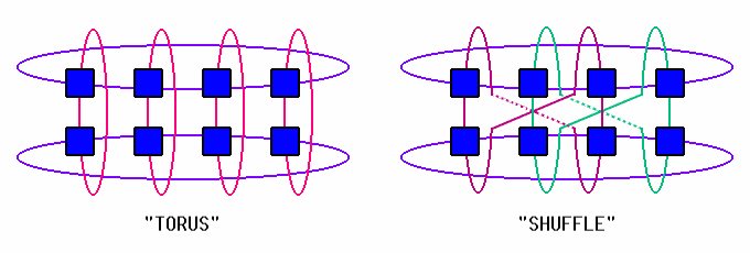
Was manufactured using a 7-layer 0.18µ CMOS8 process, consisted of 152 mln. transistors (including 137 mln. for I-cache, D-cache and S-cache) and therefore utilised a very large die size (397mm²). Prototypes were clocked at 1250MHz (TDP of 155W), though those processors installed in systems produced by HP were running at 1000MHz to 1150MHz. From the engineering point of view, EV7 couldn't stay on par with the previous representatives of the Alpha architecture considering density of functional units placed on a die, and that drawback affected the maximal core frequencies reachable, S-cache's latencies, and, in turn, performance. 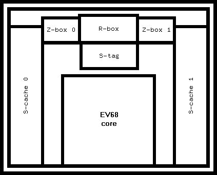
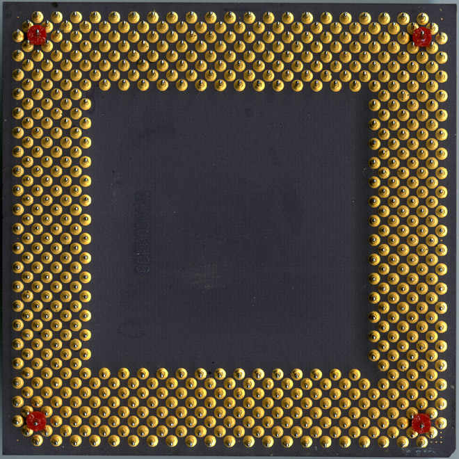
In December of 2002, HP let go out a press-release saying that first EV7-based servers would be available in January of 2003. Later, EV79 ought to be produced (using a 0.13µ SOI process), and there were no further Alpha processors planned. In March of 2003, a prototype of EV79 was observed at ISSCC with a die size of 251mm², requiring 1.2V supply, and clocked at 1450MHz (TDP of 100W). However, in October of 2003 a news about manufacturing problems sneaked out of IBM, and half a year after the processor was cancelled finally. In August of 2004, the last Alpha processor was announced, EV7z. It was clocked at 1300MHz and was manufactured using the same 0.18µ process. Like EV7, it was decided to be installed into HP's products only. There was also mentioned that servers and workstations of the Alpha architecture were subjects for sale until 2006 and for support until 2011, but no longer. 21464 (EV8), a cancelled one, was supposed to be the successor to EV7, with the number of primary functional units doubled (8 integer and 4 floating-point pipelines), and with 3Mb of S-cache. A new technology, SMT (Simultaneous Multi-Threading), should also be implemented, which meant a concurrent execution of up to 4 software streams inside of a single physical core (presumably, this technology was related somehow to HyperThreading by Intel). The die size was estimated at 420mm² for 250 mln. transistors under a 0.13µ SOI process. The initial implementation was expected to run at 1.8GHz with 1.1V core voltage (TDP of 150W). back to the contents Epilogue At the moment of writing (April of 2005), Alpha systems were offered still, mostly through HP and Microway. The latter even listed relatively inexpensive workstations based upon 21164A and AlphaPC 164LX for Linux (2000 USD for the standard configuration). Many retired, but still working workstations and servers, as well as their parts, were offered through "online flea markets". Most of those systems were working under Windows NT, and many of them would not accept neither Digital UNIX nor OpenVMS, and some even *BSD (systems with no SRM console available), though it could be still possible to install Linux under ARC/AlphaBIOS. If you have some intention to purchase an Alpha system, clarify this question before giving money unless you feel having a lack of problems. Accordingly to the statistics, DEC and Compaq sold about 800 thousand Alpha workstations and servers until June of 2001. There is no exact number how many systems have been assembled and sold by others, but estimated to be over 500 thousand. Many people say that the Alpha architecture has died on its own. Hope after passing through this article you will have no doubts that it has been buried. Alive. Because it has been more profitable to do so. There were many cases in history when a poorly crafted product prevailed over a better one. Maybe, the first product cost much less than the second one. Also possible, the second product was promoted passively too much. Maybe, licence fees were incomparable. Everything could be possible. Some would admit that marketing boys and girls promoting some goods and understanding well their poor functionality, exert themselves to the utmost extent while realising clearly that their next salary could be the last paid off otherwise. Life goes on... back to the contents Additional Information Here are Alpha-related press-releases and announcements by DEC, Compaq, Samsung asf. They have been used while writing this article, so the author assumes they may be interesting to the readers. In fact, they are history now, thus hard-to-find elsewhere. The documents are listed in chronological order. If anyone has additional ones, the author would appreciate getting their copies. 1. Digital Workstations Set New Mark for Speed, Price/Performance in Open Client/Server Computing (21-July-1994) 2. Transcript of HOTCHIPS VI Presentation of the 21164 Microprocessor (18-August-1994) 3. Digital Again Extends Performance Leadership with New Generation of Alpha AXP Microprocesors (7-September-1994) 4. Digital Microprocessor Posts World Record (7-September-1994) 5. Digital's New Alpha 21066A Chip with PCI Puts More Speed into Embedded Applications, Desktop PCs (14-November-1994) 6. Digital Extends Alpha Performance Lead with Speed Upgrades to Alpha Microprocessors (2-November-1995) 7. Newest Alpha Microprocessor Hits 500MHz, Alpha Tops for Windows NT Visual Computing (8-July-1996) 8. The 21264: A Superscalar Alpha Processor with Out-of-Order Execution (24-October-1996) 9. Alpha Is Launched into the Volume Windows NT PC Market with Low Cost 21164PC Microprocessor (17-March-1997) 10. Alpha 21164 Microprocessor Streaks to 500MHz, Sets New Industry Performance (31-March-1997) 11. Digital and Intel Announce Long-Term Agreement to Expand Relationship; Move to Settle Litigation (27-October-1997) 12. Compaq to Acquire Digital for $9.6 Billion (26-January-1998) 13. Alpha Roadmap Shows New Destinations for `98 (26-January-1998) 14. Digital to Break 1,000MHz Barrier with High-Powered New Generation of Alpha Architecture (2-February-1998) 15. Digital to Grant Samsung Architectural License for Alpha Technology (9-February-1998) 16. Samsung Introduces Alpha 21264, World's Fastest Microprocessor — Sets Standards for 64-bit Visual and Enterprise Computing (6-April-1998) 17. Samsung Targets High Performance Entry-Level Windows NT Servers; New Low-Cost Platforms Based on 500MHz to 633MHz Alpha Processors (6-April-1998) 18. Digital and Intel Complete Sale of Digital Semiconductor Manufacturing Operations (18-May-1998) 19. Alpha Processor, Inc. Debuts to Drive 64-Bit Alpha in High-Volume NT Markets (16-June-1998) 20. Samsung Electronics Develops World's First Next-Generation Wafer Processing Technology (14-September-1998) 21. Samsung Electronics Develops 0.18um Process Technology for 1GHz CPU (23-October-1998) 22. Compaq, API, and Samsung Set Long-Term Growth Strategy for Alpha (13-December-1999) 23. Compaq and Intel to Accelerate Enterprise Server Roadmaps (25-June-2001) 24. Compaq Unveils the AlphaServer ES45, Industry's Most Powerful Mid-Range Server (16-October-2001) 25. Microway Named Master Distributor and Exclusive Service Provider for API NetWorks' Alpha-Based Product Line (24-October-2001) 26. HP Introduces Most Powerful Generation of AlphaServer Systems (20-January-2003) Literature 1. Rich Witek, Dick Sites. Alpha Architecture Technical Summary, 1992. 2. Richard L. Sites. Alpha AXP Architecture, Digital Technical Journal, Vol. 4, No. 4, Special Issue, 1992. 3. Daniel W. Dobberpuhl, and others. A 200-MHz 64-bit Dual-issue CMOS Microprocessor, Digital Technical Journal, Vol. 4, No. 4, Special Issue, 1992. 4. Edward McLellan. The Alpha AXP Architecture and 21064 Processor, IEEE Micro, 1993. 5. Dina L. McKinney, and others. Digital's DECchip 21066: The First Cost-focused Alpha AXP chip, Digital Technical Journal, 1994. 6. Robert Couranz. The E2COTS System and Alpha AXP Technology: The New Computer Standard for Military Use, Digital Technical Journal, Vol. 6, No. 2, 1994. 7. Samyojita A. Nadkarni, and others. Development of Digital's PCI Chip Sets and Evaluation Kit for the DECchip 21064 Microprocessor, Digital Technical Journal, Vol. 6, No. 2, 1994. 8. Linley Gwennap. Digital Leads the Pack with 21164, Microprocessor Report, Vol. 8, No. 12, 1994. 9. William J. Bowhill, and others. Circuit Implementation of a 300-MHz 64-bit Second-generation CMOS Alpha CPU, Digital Technical Journal, Vol. 7, No. 1, 1995. 10. David P. Hunter, Eric B. Betts. Measured Effects of Adding Byte and Word Instructions to the Alpha Architecture, Digital Technical Journal, Vol. 8, No. 4, 1996. 11. Linley Gwennap. Digital, MIPS Add Multimedia Extensions, Microprocessor Report, Vol. 10, No. 15, 1996. 12. Daniel Leibholz, Rahul Razdan. The Alpha 21264: A 500 MHz Out-of-Order Execution Microprocessor, Proceedings of of IEEE COMPCON'97, 1997. 13. Michael K. Gowan, Larry L. Biro, Daniel B. Jackson. Power Considerations in the Design of the Alpha 21264 Microprocessor, DAC 98, June 15-19, 1998. 14. Linley Gwennap. Compaq, Intel Fight Digital Brain Drain, Microprocesor Report, Vol. 12, No. 14, October 26, 1998. 15. Linley Gwennap. Alpha 21364 to Ease Memory Bottleneck, Microprocessor Report, Vol. 12, No. 14, October 26, 1998. 16. M. Matson, and others. Circuit Implementation of a 600 MHz Superscalar RISC Microprocessor, Compaq Technology Journal, 1998. 17. Chart Watch: Workstation Processors, Microprocessor Report, May 10, 1999. 18. Daniel W. Bailey. High-Performance Alpha Microprocessor Design, Compaq Computer Corporation, 1999. 19. Exploring Alpha Power for Technical Computing, Compaq Technology Brief, April 2000. 20. Zarka Cvetanovic. Performance Analysis of the Alpha 21364-based HP GS1280 Multiprocessor, Hewlett-Packard Corporation, 2002. 21. Kevin Krewell. Alpha EV7 Processor: A High-Performance Tradition Continues, Microprocessor Report, April 5, 2002. 22. Ronald P. Preston. Design of an 8-wide Superscalar RISC Microprocessor with Simultaneous Multihreading, Compaq Computer Corporation, ISSCC Report, 2002. 23. Peter N. Glaskowsky. Moore, Moore, and More at ISSCC, Microprocessor Report, March 23, 2003. Many technical documents by DEC and Compaq have been used; this article wouldn't be complete without them. The author pays a credit to Wikipedia for information about DEC's early history as well as products of those old days, also to Terry Shannon for his regular and informative newsletter "Shannon Knows {DEC, Compaq, HPC}" This paper contains information collected from many unofficial Internet-resources, the full list of which is long too much to be placed below; a big and sincere appreciation goes to all their authors, for especially interesting facts, comments, points of view asf. The photographs of EV4 and EV6 are a courtesy of cpu-collector.com A special credit for extremely useful notes and suggestions made while preparing this article goes to ISA_user, VLev, Yury_Malich, Stranger_NN, and of course, to matik! (all are from forum.radeon.ru) |
|||||||||||||||||||||||||||||||||||||||